Schemes of modern power amplifiers on transistors. The simplest sound amplifier
The transistor amplifier, despite its already long history, remains a favorite subject of study for both beginners and venerable radio amateurs. And this is understandable. He is an indispensable integral part the most massive and amplifiers of low (sound) frequency. We will look at how the simplest transistor amplifiers are built.
Amplifier frequency response
In any television or radio receiver, in every music center or sound amplifier, you can find transistor sound amplifiers (low frequency - LF). The difference between audio transistor amplifiers and other types lies in their frequency response.
The transistor audio amplifier has a uniform frequency response in the frequency band from 15 Hz to 20 kHz. This means that all input signals with a frequency within this range are converted (amplified) by the amplifier in approximately the same way. The figure below shows the ideal frequency response curve for an audio amplifier in the coordinates "amplifier gain Ku - input signal frequency".
This curve is almost flat from 15 Hz to 20 kHz. This means that such an amplifier should be used specifically for input signals with frequencies between 15 Hz and 20 kHz. For input signals above 20 kHz or below 15 Hz, the efficiency and quality of its performance rapidly decrease.
The type of frequency response of the amplifier is determined by the electrical radio elements (ERE) of its circuit, and above all by the transistors themselves. An audio amplifier based on transistors is usually assembled on the so-called low- and mid-frequency transistors with a total bandwidth of input signals from tens and hundreds of Hz to 30 kHz.
Amplifier class
As you know, depending on the degree of continuity of the current flow throughout its period through the transistor amplifying stage (amplifier), the following classes of its operation are distinguished: "A", "B", "AB", "C", "D".
In the class of operation, current "A" flows through the stage for 100% of the period of the input signal. The operation of the cascade in this class is illustrated in the following figure.

In the class of operation of the amplifier stage "AB", the current flows through it for more than 50%, but less than 100% of the period of the input signal (see figure below).

In the class of operation of the "B" stage, the current flows through it exactly 50% of the period of the input signal, as illustrated in the figure.

And finally, in the class of operation of the "C" stage, the current through it flows less than 50% of the period of the input signal.
Low-frequency amplifier on transistors: distortion in the main classes of work
In the working area, a class "A" transistor amplifier has a low level of non-linear distortion. But if the signal has impulse surges in voltage, leading to saturation of the transistors, then higher harmonics (up to the 11th) appear around each “standard” harmonic of the output signal. This causes the phenomenon of the so-called transistorized or metallic sound.
If low-frequency power amplifiers on transistors have an unstabilized power supply, then their output signals are modulated in amplitude near the mains frequency. This leads to harshness of the sound at the left edge of the frequency response. Various methods of voltage stabilization make the design of the amplifier more complex.
typical efficiency single ended amplifier class A does not exceed 20% due to the constantly open transistor and the continuous flow of the direct current component. You can make a class A amplifier push-pull, the efficiency will increase slightly, but the half-waves of the signal will become more asymmetric. The transfer of the cascade from the work class "A" to the work class "AB" quadruples the nonlinear distortion, although the efficiency of its circuit increases.
In amplifiers of classes "AB" and "B", distortion increases as the signal level decreases. You involuntarily want to turn up such an amplifier louder to complete the sensations of the power and dynamics of the music, but often this does not help much.
Intermediate classes of work
The class of work "A" has a variety - the class "A +". In this case, the low-voltage input transistors of the amplifier of this class operate in class "A", and the high-voltage output transistors of the amplifier, when their input signals exceed a certain level, go into classes "B" or "AB". The efficiency of such cascades is better than in the pure class "A", and the non-linear distortion is less (up to 0.003%). However, their sound is also "metallic" due to the presence of higher harmonics in the output signal.
For amplifiers of another class - "AA" the degree of nonlinear distortion is even lower - about 0.0005%, but higher harmonics are also present.
A return to a class "A" transistor amplifier?
Today, many experts in the field of high-quality sound reproduction advocate a return to tube amplifiers, since the level of non-linear distortion and higher harmonics introduced by them into the output signal is obviously lower than that of transistors. However, these advantages are largely offset by the need for a matching transformer between the high-impedance tube output stage and the low-impedance speakers. However, a simple transistorized amplifier can also be made with a transformer output, as will be shown below.
There is also a point of view that only a hybrid tube-transistor amplifier can provide the ultimate sound quality, all stages of which are single-ended, not covered and work in class "A". That is, such a power follower is an amplifier on a single transistor. Its scheme can have the maximum achievable efficiency (in class "A") no more than 50%. But neither the power nor the efficiency of the amplifier are indicators of the quality of sound reproduction. Wherein special meaning acquire the quality and linearity of the characteristics of all ERE in the circuit.
Since single-ended circuits are gaining this perspective, we will look at their options below.
single-ended amplifier with one transistor
Its circuit, made with a common emitter and R-C connections for input and output signals for operation in class "A", is shown in the figure below.

It shows the npn transistor Q1. Its collector is connected to the +Vcc positive terminal via a current-limiting resistor R3, and its emitter is connected to -Vcc. transistor amplifier p-n-p structures will have the same circuit, but the power supply leads will be reversed.
C1 is a decoupling capacitor, by means of which the source of the alternating input signal is separated from the source constant voltage Vcc. At the same time, C1 does not prevent the passage of an alternating input current through the base-emitter junction of transistor Q1. Resistors R1 and R2, together with the resistance of the "E - B" junction, form Vcc to select the operating point of the transistor Q1 in static mode. Typical for this circuit is the value of R2 = 1 kOhm, and the position of the operating point is Vcc / 2. R3 is the load resistor of the collector circuit and is used to create a variable voltage output signal on the collector.
Assume that Vcc = 20 V, R2 = 1 kΩ, and the current gain h = 150. We select the emitter voltage Ve = 9 V, and the voltage drop at the E-B junction is Vbe = 0.7 V. This value corresponds to the so-called silicon transistor. If we were considering an amplifier based on germanium transistors, then the voltage drop across the open E-B junction would be Vbe = 0.3 V.
Emitter current, approximately equal to collector current
Ie = 9 V/1 kΩ = 9 mA ≈ Ic.
Base current Ib = Ic/h = 9 mA/150 = 60 µA.
Voltage drop across resistor R1
V(R1) = Vcc - Vb = Vcc - (Vbe + Ve) = 20V - 9.7V = 10.3V,
R1 \u003d V (R1) / Ib \u003d 10.3 V / 60 μA \u003d 172 kOhm.
C2 is needed to create a circuit for the passage of the variable component of the emitter current (actually the collector current). If it were not there, then the resistor R2 would severely limit the variable component, so that the bipolar transistor amplifier in question would have a low current gain.
In our calculations, we assumed that Ic = Ib h, where Ib is the base current flowing into it from the emitter and arising when a bias voltage is applied to the base. However, through the base always (both with and without bias) the leakage current from the collector Icb0 also flows. Therefore, the real collector current is Ic = Ib h + Icb0 h, i.e. the leakage current in the circuit with OE is amplified by 150 times. If we were considering an amplifier based on germanium transistors, then this circumstance would have to be taken into account in the calculations. The fact is that they have a significant Icb0 of the order of several μA. In silicon, it is three orders of magnitude smaller (about a few nA), so it is usually neglected in calculations.
Single ended amplifier with MIS transistor
Like any field-effect transistor amplifier, the circuit under consideration has its own analogue among amplifiers. Therefore, we will consider an analogue of the previous circuit with a common emitter. It is made with a common source and R-C connections for input and output signals for operation in class "A" and is shown in the figure below.

Here C1 is the same decoupling capacitor, by means of which the source of the alternating input signal is separated from the source of the constant voltage Vdd. As you know, any field-effect transistor amplifier must have the gate potential of its MIS transistors below the potentials of their sources. In this circuit, the gate is grounded by R1, which is typically high resistance (100 kΩ to 1 MΩ) so that it does not shunt the input signal. There is practically no current through R1, so the gate potential in the absence of an input signal is equal to the ground potential. The source potential is higher than the ground potential due to the voltage drop across the resistor R2. Thus, the gate potential is lower than the source potential, which is necessary for normal operation of Q1. Capacitor C2 and resistor R3 have the same purpose as in the previous circuit. Since this is a common-source circuit, the input and output signals are out of phase by 180°.
Amplifier with transformer output
The third single-stage simple transistor amplifier, shown in the figure below, is also made according to the common emitter circuit for operation in class "A", but it is connected to a low-impedance speaker through a matching transformer.

The primary winding of the transformer T1 is the load of the collector circuit of the transistor Q1 and develops the output signal. T1 sends the output signal to the speaker and ensures that the output impedance of the transistor matches the low (on the order of a few ohms) speaker impedance.
The voltage divider of the collector power supply Vcc, assembled on resistors R1 and R3, provides the choice of the operating point of the transistor Q1 (supplying a bias voltage to its base). The purpose of the remaining elements of the amplifier is the same as in the previous circuits.
Push-Pull Audio Amplifier
A two-transistor push-pull low-frequency amplifier splits the input frequency into two anti-phase half-waves, each of which is amplified by its own transistor stage. After such amplification is performed, the half-waves are combined into an integral harmonic signal, which is transmitted to acoustic system. Such a conversion of the low-frequency signal (splitting and re-merging), of course, causes irreversible distortion in it, due to the difference in the frequency and dynamic properties of the two transistors of the circuit. These distortions reduce the sound quality at the output of the amplifier.
Push-pull amplifiers operating in class "A" do not reproduce complex audio signals well enough, since there is a continuous flow in their shoulders D.C. elevated size. This leads to asymmetry of the half-waves of the signal, phase distortions and, ultimately, to the loss of sound intelligibility. When heated, two powerful transistors double the signal distortion in the low and infra low frequencies. But still, the main advantage of the push-pull circuit is its acceptable efficiency and increased output power.
A push-pull transistor power amplifier circuit is shown in the figure.

This is an amplifier for class "A", but class "AB" and even "B" can also be used.
Transformerless Transistor Power Amplifier
Transformers, despite the success in their miniaturization, are still the most bulky, heavy and expensive ERE. Therefore, a way was found to eliminate the transformer from the push-pull circuit by performing it on two powerful complementary transistors. different types(n-p-n and p-n-p). Most modern power amplifiers use this principle and are designed to operate in class "B". A diagram of such a power amplifier is shown in the figure below.

Both of its transistors are connected according to a common collector (emitter follower) circuit. Therefore, the circuit transfers the input voltage to the output without amplification. If there is no input signal, then both transistors are on the border of the on state, but they are turned off.
When a harmonic signal is input, its positive half-wave opens TR1, but translates pnp transistor TR2 is fully into cutoff mode. Thus, only the positive half-wave of the amplified current flows through the load. The negative half-wave of the input signal opens only TR2 and turns off TR1, so that the negative half-wave of amplified current is supplied to the load. As a result, a full power amplified (due to current amplification) sinusoidal signal is emitted at the load.
Single transistor amplifier
To assimilate the above, we will assemble a simple transistor amplifier with our own hands and figure out how it works.
As a load of a low-power transistor T of type BC107, we turn on headphones with a resistance of 2-3 kOhm, we supply the bias voltage to the base from a high-resistance resistor R* of 1 MΩ, which decouples an electrolytic capacitor C with a capacity of 10 μF to 100 μF, we include it in the base circuit T. Feed the circuit we will be from a 4.5 V / 0.3 A battery.

If resistor R* is not connected, then there is neither base current Ib nor collector current Ic. If the resistor is connected, then the voltage at the base rises to 0.7 V and the current Ib = 4 μA flows through it. The current gain of the transistor is 250, which gives Ic = 250Ib = 1 mA.
Having assembled a simple transistor amplifier with our own hands, we can now test it. Connect the headphones and place your finger on point 1 of the diagram. You will hear a noise. Your body perceives the radiation of the mains at a frequency of 50 Hz. The noise you hear from the headphones is this radiation, only amplified by the transistor. Let us explain this process in more detail. An AC voltage of 50 Hz is connected to the base of the transistor through capacitor C. The voltage at the base is now equal to the sum of the DC bias voltage (approximately 0.7 V) coming from the resistor R* and the finger AC voltage. As a result, the collector current receives an alternating component with a frequency of 50 Hz. This alternating current is used to move the diaphragm of the speakers back and forth at the same frequency, which means we can hear a 50Hz tone at the output.
Listening to the 50 Hz noise level is not very interesting, so you can connect low-frequency signal sources (CD player or microphone) to points 1 and 2 and hear amplified speech or music.
I must say right away that the assembly of this amplifier is justified only as an experiment, since the sound quality will, at best, be at the level of cheap Chinese receivers - scanners. If someone wants to build himself a low-power amplifier with more high-quality sound, using microchip TDA 2822m , you can go to the following link:
Portable speaker for a player or phone on a tda2822m chip
Amplifier test photo:
The following figure lists the required parts: 
Almost any of the medium and high power bipolar transistors can be used in the circuit. n-p-n structures, for example, KT 817. It is desirable to put a film capacitor at the input, with a capacity of 0.22 - 1 μF. An example of film capacitors in the following photo:
I bring a drawing printed circuit board from the program Sprint layout : 
The signal is taken from the output of an mp3 player or telephone, ground and one of the channels are used. In the following figure, you can see the wiring diagram for the Jack 3.5 plug, for connecting to a signal source:
If desired, this amplifier, like any other, can be equipped with a volume control by connecting a 50 KΩ potentiometer according to the standard scheme, 1 channel is used:
Parallel to the power supply, if the power supply after diode bridge it is not worth a large-capacity electrolytic capacitor, you need to put an electrolyte at 1000 - 2200 uF, with an operating voltage greater than the supply voltage of the circuit.
An example of such a capacitor:
You can download the printed circuit board of an amplifier on a single transistor for the sprint-layout program in the My files section of the site.
You can evaluate the sound quality of this amplifier by watching the video of its work on our channel.
The editors of the site "Two Schemes" presents a simple, but quality amplifier LF on MOSFET transistors. His circuit should be well known to audiophile radio amateurs, since she is already 20 years old. The circuit is the development of the famous Anthony Holton, which is why it is sometimes called ULF Holton. The sound amplification system has low harmonic distortion, not exceeding 0.1%, with a power load of about 100 watts.
This amplifier is an alternative to the popular amplifiers of the TDA series and similar pop ones, because at a slightly higher cost you can get an amplifier with clearly better characteristics.
The big advantage of the system is simple design and an output stage consisting of 2 inexpensive MOSFETs. The amplifier can drive both 4 and 8 ohm speakers. The only adjustment that needs to be made during startup is to set the quiescent current value of the output transistors.
Schematic diagram of UMZCH Holton
 Holton amplifier on MOSFET - circuit
 The circuit is a classic two-stage amplifier, it consists of a differential input amplifier and a balanced power amplifier, in which one pair of power transistors operates. The scheme of the system is presented above.
Printed circuit board


 ULF printed circuit board - finished view
 Here is the archive from PDF files printed circuit board - .
The principle of operation of the amplifier
Transistors T4 (BC546) and T5 (BC546) operate in a differential amplifier configuration and are powered by a current source built on the basis of transistors T7 (BC546), T10 (BC546) and resistors R18 (22 kohm), R20 (680 ohms) and R12 (22 com). The input signal is fed to two filters: a low-pass filter, built from the elements R6 (470 ohms) and C6 (1 nf) - it limits the high-frequency components of the signal and a band-pass filter, consisting of C5 (1 uF), R6 and R10 (47 kΩ), limiting signal components at infra-low frequencies.
The load of the differential amplifier is resistors R2 (4.7 kohm) and R3 (4.7 kohm). Transistors T1 (MJE350) and T2 (MJE350) are another amplification stage, and transistors T8 (MJE340), T9 (MJE340) and T6 (BD139) are its load.
Capacitors C3 (33pF) and C4 (33pF) counteract the excitation of the amplifier. Capacitor C8 (10 nF) connected in parallel with R13 (10 kΩ/1 V) improves transient response ULF, which is important for rapidly rising input signals.
Transistor T6, together with the elements R9 (4.7 kohm), R15 (680 ohms), R16 (82 ohms) and PR1 (5 ohms), allows you to set the correct polarity of the output stages of the amplifier at rest. Using a potentiometer, it is necessary to set the quiescent current of the output transistors within 90-110 mA, which corresponds to a voltage drop across R8 (0.22 ohm / 5 W) and R17 (0.22 ohm / 5 W) within 20-25 mV. The total current consumption in the rest mode of the amplifier should be in the region of 130 mA.
The output elements of the amplifier are MOSFETs T3 (IRFP240) and T11 (IRFP9240). These transistors are installed as a voltage follower with a large maximum output current, so the first 2 stages must swing a large enough amplitude for the output signal.
Resistors R8 and R17 were mainly used to quickly measure the quiescent current of power amplifier transistors without interfering with the circuit. They may also come in handy if the system is expanded with another pair of power transistors, due to differences in resistance. open channels transistors.
Resistors R5 (470 ohms) and R19 (470 ohms) limit the charging rate of the capacitance of the pass transistors, and, therefore, limit frequency range amplifier. Diodes D1-D2 (BZX85-C12V) protect powerful transistors. With them, the voltage at startup relative to power supplies for transistors should not be more than 12 V.
The amplifier board provides places for power filter capacitors C2 (4700 uF / 50 V) and C13 (4700 uF / 50 V).
 Homemade transistor ULF on MOSFET
 The control is powered through an additional RC filter built on the elements R1 (100 ohm / 1 V), C1 (220 μF / 50 V) and R23 (100 Ω / 1 V) and C12 (220 μF / 50 V).
Power supply for UMZCH
The amplifier circuit provides power that reaches a real 100 watts (effective sinusoidal), with an input voltage in the region of 600 mV and a load resistance of 4 ohms.
 Amplifier Holton on the board with details
 The recommended transformer is a 200 W toroid with a voltage of 2x24 V. After rectification and smoothing, you should get a two-polar supply to the power amplifiers in the region of +/-33 Volts. The design shown here is a very good performance MOSFET mono amplifier module that can be used as a standalone unit or as part of a .
Low frequency amplifiers (ULF) are used to convert weak signals predominantly in the audio range into more powerful signals acceptable for direct perception through electrodynamic or other sound emitters.
Note that high-frequency amplifiers up to frequencies of 10 ... 100 MHz are built according to similar schemes, the whole difference most often comes down to the fact that the values of the capacitances of the capacitors of such amplifiers decrease as many times as the frequency of the high-frequency signal exceeds the frequency of the low-frequency one.
A simple single transistor amplifier
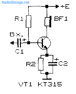
The simplest ULF, made according to the scheme with a common emitter, is shown in Fig. 1. A telephone capsule was used as a load. The allowable supply voltage for this amplifier is 3 ... 12 V.
It is desirable to determine the value of the bias resistor R1 (tens of kΩ) experimentally, since its optimal value depends on the supply voltage of the amplifier, the resistance of the telephone capsule, and the transmission coefficient of a particular instance of the transistor.
Rice. 1. Scheme of a simple ULF on one transistor + capacitor and resistor.
For selection initial value resistor R1 should be taken into account that its value is about a hundred or more times greater than the resistance included in the load circuit. To select a bias resistor, it is recommended to connect in series a constant resistor with a resistance of 20 ... 30 kOhm and a variable resistor with a resistance of 100 ... 1000 kOhm, after which, applying to the input of the amplifier sound signal small amplitude, for example, from a tape recorder or player, by turning the variable resistor knob to achieve best quality signal at its highest volume.
The value of the capacitance of the transition capacitor C1 (Fig. 1) can be in the range from 1 to 100 microfarads: the greater the value of this capacitance, the lower frequencies the ULF can amplify. To master the technique of amplifying low frequencies, it is recommended to experiment with the selection of the values of the elements and the operating modes of the amplifiers (Fig. 1 - 4).
Improved Single Transistor Amplifier Options
Complicated and improved in comparison with the scheme in fig. 1 amplifier circuits are shown in fig. 2 and 3. In the diagram in fig. 2 amplification stage additionally contains a chain of frequency-dependent negative feedback(resistor R2 and capacitor C2), which improves the signal quality.
Rice. 2. Scheme of a single-transistor ULF with a chain of frequency-dependent negative feedback.

Rice. 3. A single-transistor amplifier with a divider to supply a bias voltage to the base of the transistor.

Rice. 4. Single transistor amplifier with automatic bias setting for the base of the transistor.
In the diagram in fig. 3, the bias to the base of the transistor is set more “rigidly” using a divider, which improves the quality of the amplifier when its operating conditions change. An “automatic” bias setting based on an amplifying transistor is used in the circuit in fig. four.
Two-stage transistor amplifier
By connecting in series two simple amplification stages (Fig. 1), you can get a two-stage ULF (Fig. 5). The gain of such an amplifier is equal to the product of the gains of the individual stages. However, it is not easy to obtain a large stable gain with a subsequent increase in the number of stages: the amplifier will most likely self-excite.
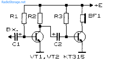
Rice. 5. Scheme of a simple two-stage bass amplifier.
New developments of low-frequency amplifiers, the circuits of which are often cited on the pages of magazines in recent years, are aimed at achieving a minimum coefficient of non-linear distortion, increasing output power, expanding the bandwidth of amplified frequencies, etc.
At the same time, when setting up various devices and conducting experiments, a simple ULF is often needed, which can be assembled in a few minutes. Such an amplifier should contain a minimum number of deficient elements and operate in a wide range of supply voltage and load resistance.
ULF circuit on field-effect and silicon transistors
A diagram of a simple low-frequency power amplifier with a direct connection between the cascades is shown in fig. 6 [Rl 3/00-14]. The input impedance of the amplifier is determined by the value of the potentiometer R1 and can vary from hundreds of ohms to tens of megohms. The output of the amplifier can be connected to a load with a resistance of 2 ... 4 to 64 ohms and higher.
With a high-resistance load, the KT315 transistor can be used as VT2. The amplifier is operable in the supply voltage range from 3 to 15 V, although its acceptable performance is maintained even when the supply voltage drops down to 0.6 V.
Capacitor C1 can be selected from 1 to 100 microfarads. In the latter case (C1 \u003d 100 μF), the ULF can operate in the frequency band from 50 Hz to 200 kHz and above.

Rice. 6. Scheme of a simple low-frequency amplifier on two transistors.
The amplitude of the ULF input signal should not exceed 0.5 ... 0.7 V. The output power of the amplifier can vary from tens of mW to units of W, depending on the load resistance and the magnitude of the supply voltage.
Setting up the amplifier consists in selecting resistors R2 and R3. With their help, the voltage at the drain of the transistor VT1 is set, equal to 50 ... 60% of the voltage of the power source. Transistor VT2 must be installed on a heat sink plate (radiator).
Track-cascade ULF with direct connection
On fig. 7 shows a diagram of another outwardly simple ULF with direct connections between cascades. This kind of communication improves frequency characteristics amplifier in the low-frequency region, the circuit as a whole is simplified.

Rice. 7. circuit diagram three-cascade ULF with direct connection between the cascades.
At the same time, the tuning of the amplifier is complicated by the fact that each amplifier resistance has to be selected individually. Roughly, the ratio of resistors R2 and R3, R3 and R4, R4 and R BF should be within (30 ... 50) to 1. Resistor R1 should be 0.1 ... 2 kOhm. The calculation of the amplifier shown in fig. 7 can be found in the literature, eg [P 9/70-60].
Schemes of cascade ULF on bipolar transistors
On fig. 8 and 9 show cascode ULF circuits on bipolar transistors. Such amplifiers have a rather high gain Ku. The amplifier in fig. 8 has Ku=5 in the frequency band from 30 Hz to 120 kHz [MK 2/86-15]. ULF according to the scheme in Fig. 9 with a harmonic coefficient of less than 1% has a gain of 100 [RL 3/99-10].

Rice. 8. Cascade ULF on two transistors with gain = 5.

Rice. 9. Cascade ULF on two transistors with gain = 100.
Economical ULF on three transistors
For portable electronic equipment, an important parameter is the efficiency of VLF. The scheme of such a ULF is shown in fig. 10 [RL 3/00-14]. Here, a cascade connection of a field-effect transistor VT1 and a bipolar transistor VT3 is used, and the transistor VT2 is turned on in such a way that it stabilizes the operating point of VT1 and VT3.
With an increase in the input voltage, this transistor shunts the emitter-base VT3 junction and reduces the value of the current flowing through the transistors VT1 and VT3.

Rice. 10. Scheme of a simple economical low-frequency amplifier on three transistors.
As in the above circuit (see Fig. 6), the input impedance of this ULF can be set in the range from tens of ohms to tens of megohms. A telephone primer, for example, TK-67 or TM-2V, was used as a load. A telephone capsule connected with a plug can simultaneously serve as a power switch for the circuit.
The ULF supply voltage ranges from 1.5 to 15 V, although the device remains operational even when the supply voltage drops to 0.6 V. In the supply voltage range of 2 ... 15 V, the current consumed by the amplifier is described by the expression:
1(µA) = 52 + 13*(Upit)*(Upit),
where Upit is the supply voltage in Volts (V).
If you turn off the transistor VT2, the current consumed by the device increases by an order of magnitude.
Two-cascade ULF with direct connection between the cascades
Examples of ULF with direct connections and a minimum selection of the operating mode are the circuits shown in Fig. 11 - 14. They have high gain and good stability.

Rice. 11. A simple two-stage ULF for a microphone (low noise level, high gain).

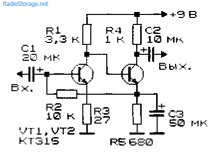
Rice. 12. Two-stage low-frequency amplifier based on KT315 transistors.
Rice. 13. Two-stage low-frequency amplifier based on KT315 transistors - option 2.
The microphone amplifier (Fig. 11) is characterized by a low level of intrinsic noise and a high gain [MK 5/83-XIV]. An electrodynamic type microphone was used as the BM1 microphone.
A telephone capsule can also act as a microphone. Stabilization of the operating point (initial bias based on the input transistor) of the amplifiers in fig. 11 - 13 is carried out due to the voltage drop across the emitter resistance of the second amplification stage.

Rice. 14. Two-stage ULF with a field-effect transistor.
The amplifier (Fig. 14), which has a high input resistance (about 1 MΩ), is made on a field-effect transistor VT1 (source follower) and bipolar - VT2 (with a common one).
A cascade low-frequency field-effect transistor amplifier, which also has a high input impedance, is shown in fig. fifteen.

Rice. 15. diagram of a simple two-stage ULF on two field-effect transistors.
ULF circuits for working with low-ohm load
Typical ULF designed to operate on a low-resistance load and having output power tens of mW and higher are shown in Fig. 16, 17.

Rice. 16. A simple ULF for working with a low-resistance load.
Electrodynamic head BA1 can be connected to the output of the amplifier, as shown in fig. 16, or in the diagonal of the bridge (Fig. 17). If the power source is made of two batteries (accumulators) connected in series, the output of the BA1 head, right according to the diagram, can be connected to their midpoint directly, without capacitors C3, C4.

Rice. 17. Low-frequency amplifier circuit with the inclusion of a low-resistance load in the diagonal of the bridge.
If you need a circuit for a simple tube ULF, then such an amplifier can be assembled even on a single tube, see our electronics website in the appropriate section.
Literature: Shustov M.A. Practical Circuitry (Book 1), 2003.
Corrections in the post: in fig. 16 and 17 instead of the diode D9, a chain of diodes is installed.
- 20.09.2014
The rating of passive components for surface mounting is marked according to certain standards and does not directly correspond to the numbers printed on the case. The article introduces these standards and will help you avoid mistakes when replacing chip components. basis of production modern means electronic and computer science is surface mount technology or SMT technology (SMT - Surface Mount Technology). …
- 21.09.2014
The figure shows a diagram of a simple touch switch on the IC 555. The 555 timer operates in comparator mode. When the plates touch, the comparator switches, which in turn controls the open-collector transistor VT1. An external load can be connected to the "open" collector, powered by an external or internal power source, external power …
- 12.12.2015
in the preamplifier for dynamic microphone uA739 dual op amp is used. Both channels of the preamplifier are the same, so only one is shown in the diagram. A 50% supply voltage is applied to the non-inverting input of the op-amp, which is set by resistors R1 and R4 (voltage divider), while this voltage is used simultaneously by two amplifier channels. The R3C3 circuit is...
- 23.09.2014
Watches with a static display have a brighter glow of the indicators compared to dynamic indication, the diagram of such a clock is shown in Figure 1. The indicator control device is the K176ID2 decoder, this microcircuit will provide a sufficiently high brightness of the glow LED indicator. K561IE10 microcircuits are used as counters, each contains 20a of four bits ...


